How Microchips Are Made: Design, Fabrication, and Packaging Processes
Learn how microchips are designed and fabricated through wafer processing, front-end and back-end manufacturing, and advanced semiconductor technologies.
The integrated circuit (IC), or microchip, was invented by Jack Kilby in 1958. There are many types of microchips. Microprocessors are logic chips that are used to perform computations (binary codes, logic gates, Boolean algebra, etc.). Memory chips, such as NAND (Not AND), store data. Analog chips operate over a continuous range of signal. Analog chips can be subdivided into linear IC and radio frequency IC. Digital signal processors convert between analog and digital signals.
Application-specific ICs (ASICs) are customized chips for a special purpose. They are used in cars, televisions, digital cameras, or appliances and more.
Based on a microchip's feature and development plan that encompasses use, power, area, cost, time to market, an IC's function and performance are determined and the logic circuit is designed.
During logic circuit design, a logic circuit diagram is drawn to determine the electronic circuit required for performing requested functions. Once the logic circuit diagram is complete, simulations are performed multiple times to test the circuit's operation. If there is no issue with the operation, the actual layout pattern for the devices and interconnects is designed by computer-aided design (Figure 1).
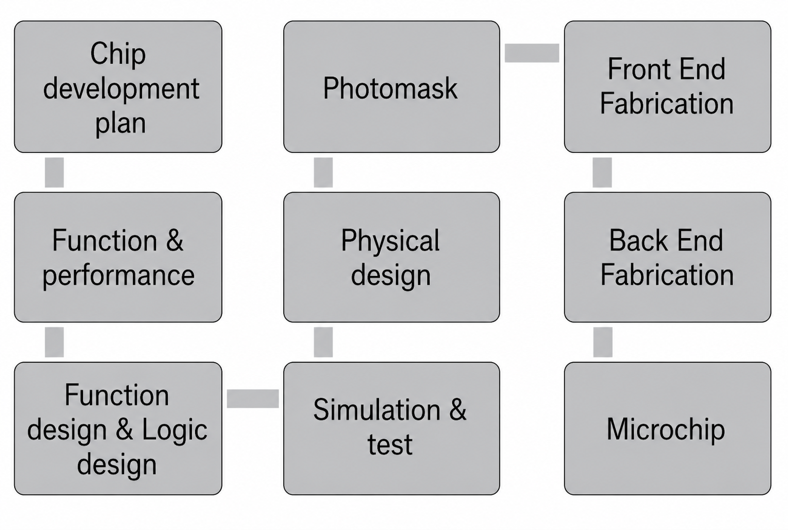
Figure 1 IC design and fabrication.
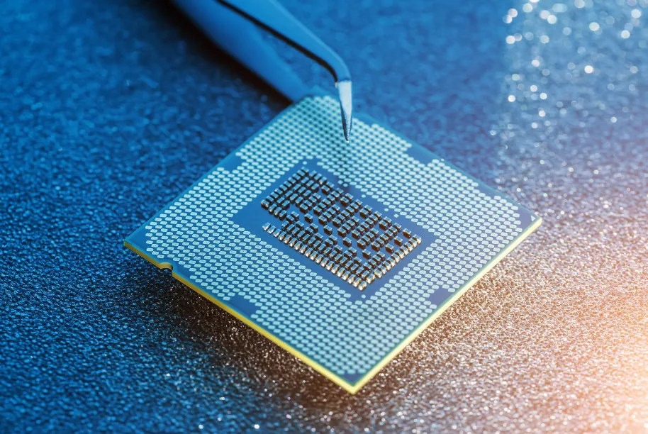
How A Microchip is Made
A sophisticated processor can contain hundreds of millions or billions of transistors interconnected by fine metal wires. The process of making chips is extremely complex requiring hundreds of precisely controlled steps.
The base material of microchips is silicon. Silicon is called a semiconductor that relates to its molecular structure. Silicon can conduct electricity under certain conditions and nonconductive under others. This feature acts as a basic circuit of a transistor: an on/off or binary 1/0 switches either allowing or preventing electrical current to pass through a gate. The process of manufacturing microchips building millions or billions of transistors on an IC chip makes it phenomenally precise and complex.
The process of manufacturing microchips includes following three main processes:
(1) wafer manufacturing
(2) front-end of line processing, and
(3) back-end of line processing.
A microchip is formed by more than hundreds repetitive operations during front-end of line processing (Figure 2). The process of manufacturing IC chip is supported by advanced manufacturing technologies that encompass material handling automation, computer-integrated-manufacturing, advanced process control, manufacturing execution system, etc.
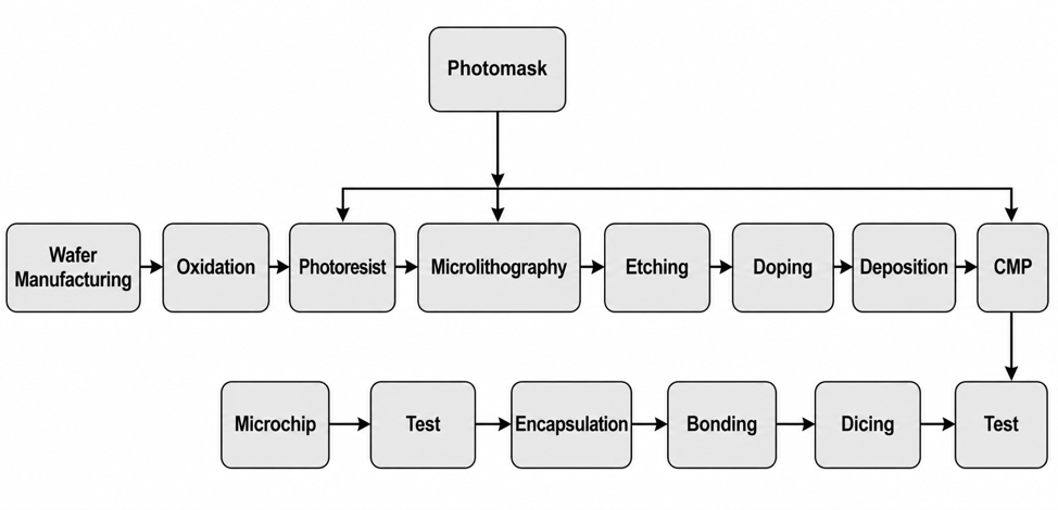
Figure 2 Wafer manufacturing, photomask, front-end of line process, and back-end of line process.
In the fabrication of IC, wafer serves as a substrate for IC to build-on. Many steps in front-end processing, including oxidation, photolithography, etching, doping, deposition of various materials, are built over the wafer in accordance with the IC design. Inspection and testing are also included in each step of the processes. Finally, the dies are cut, packaged, tested, and ready to be used.
1. Wafer Manufacturing
A wafer, also called a slice or substrate, is a thin disc (about thickness of a credit card) made of silicon, or other semiconductor materials such as GaAs. Silicon, the principal ingredient in beach sand, is the second most abundant element in the earth after oxygen. Before it can be used in semiconductor manufacturing it is refined to nearly 100 percent pure.
1.1 Silicon Ingot
Semiconductor manufacturing begins with a silicon ingot. Silicon ingots could be made by Czochralski (CZ) process and float-zone process.
Float-zone wafers are generally not larger than 150 mm due to limit of surface tension during growing process. Most crystal ingots are grown by the Czochralski method. This method begins by a piece of crystal of silicon, called seed, is lowered in the near 100 percent pure molten silicon in crucible. The seed and crucible are rotating in opposite direction while heating purified silicon to 1200°C in an argon atmosphere. The silicon seed is slowly withdrawn from molten liquid. Silicon atoms attach to the seed, resulting in a long crystal rod or ingot, grows with a diameter of most commonly 200 or 300-millimeter (mm) across in careful control of temperature, atmosphere, and pressures. It produces electronic grade silicon that is semiconductor manufacturing quality with silicon purity to 99.9999999 percent.
1.2 Wafer Fabrication Process
A series of operations is performed to prepare silicon wafers from a silicon ingot.
Cropping, Grinding, Slicing
The ends of single crystal ingot are cropped using a single-bladed diamond saw with water coolant. The ingot is then ground to a uniform diameter and the ends are chamfered to reduce the possibility of shattering the ingot. The crystal structure is determined by x-ray diffraction. A longitudinal flat section is produced by wet grinding to indicate crystal orientation of the ingot. Ingots are sliced into discs or called substrates.
Lapping
After slicing, the wafers are mechanically lapped under pressure on both sides of the wafer in order to achieve flatness and parallelism. Lapping operations will remove the surface silicon which has been damaged by the slicing process and thin the wafer to desired thickness. The edge of the individual wafer is rounded by the use of wet automatic grinders.
Etching
Wafer dicing and lapping degrade the silicon surface crystal structure, so wafers are etched with a solution containing nitric, acetic, or hydrofluoric acids in order to remove external damaged surface and reduce the thickness of the wafer. Etching operation could be done in manual etch tanks or automated etching machines.
Polishing
After etching, the wafers are polished to a super-flat, flawless, and mirror-smooth surface with remaining roughness at atomic scale. Polishing process is usually completed in two or three polishing steps. Wafers are mounted onto a metal carrier plate that is attached to the polishing machine by vacuum. The polishing process combines with pressure mechanically and chemically using fine slurry such as Al2O3, SiO2, or CeO2.
Cleaning
Finally, the wafers are cleaned to remove any particles on the surface of a polished wafer thereby making the wafer residual free. Variable ultrapure chemicals could be used for cleaning that include ammonia, hydrogen peroxide, hydrofluoric acid, hydrochloric acid, and deionized water.
2. Front-End of Line Processing
Building circuits on a wafer is an extremely complex and precise process. The process consists of hundreds of precisely controlled steps with as many as 30 layers of complex circuitry. Chips are built, taking from 10 to 30 days or more, in specific patterns and recipes to produce hundreds or thousands of die on each 300-mm wafer.
The process of making IC chips is called fabrication. The factories where chips are made are called fabrication facility or fab. In a fab, there are cleanrooms where fabrication in batch of wafers is built. Because particles of dust can ruin the complex circuitry on a chip, purified air is constantly recirculated in a cleanroom.
For a class ISO 1 cleanroom, a cubic meter of air contains no more than 10 particles, measuring 0.1 micrometer or μm (millionth of a meter). Fab technicians wear bunny suits that are specially designed to keep contaminants off the wafers during fabrication.
The following are operations in the Front End of Line Processing (FEOL).
2.1 Epitaxy
Epitaxy is one of the fundamental processes used to make semiconductor devices. Epitaxy refers to deposit an overlayer of a crystal (epitaxial film) on a host crystal (substrate) in an ordered fashion. It is desired that the overlayer has a defined orientation with respect to the substrate. The epitaxial film and substrate could be same or different materials. There are three types of epitaxy: liquid phase, vapor phase, and molecular beam epitaxy.
2.2 Oxidization
Silicon oxide (SiO2) serves as an electrical insulator that is a key component in IC circuit. Growth of oxidation can be achieved by dry or wet oxidation.
Oxidation is a diffusion process. Silicon wafers are first heated and exposed to ultrapure oxygen at elevated temperatures in a diffusion furnace. By carefully controlled conditions in the furnace, a silicon oxide (SiO2) film, dry oxidation, with uniform thickness is growth from the SiO2/silicon interface.
$$\text{Si} + \text{O}_2 \rightarrow \text{SiO}_2$$
Wet oxidation is preferred to dry oxidation for growing thicker oxide at a faster rate. Wet oxidation is performed by exposing the wafer to ultra-high-purity water vapor or using hydrogen and oxygen which are burned in a torch flame to form ultra-high-purity water vapor in an oxidizing furnace.
$$\text{Si} + 2\text{H}_2\text{O} \rightarrow \text{SiO}_2 + 2\text{H}_2$$
2.3 Photolithography
Photolithography is a process by imprinting a specific IC design pattern on a wafer. Before performing the photolithography process, a photomask (reticle) is prepared. A photomask has a copy of the circuit pattern drawn as an opaque pattern on a quartz plate. A quartz plate is first polished in high precision. The quartz substrate is then coated with a thin layer of chrome material by sputtering that is opaque to UV wavelengths.
A photosensitive chemical called resist is spin-coated over the chrome photomask blank. Then a circuit design pattern is transcribed into the chrome film by electron beam lithography. After exposure, develop and etch, the photomask blank becomes a photomask with a copy of the circuit pattern.
Photoresist Application
A wafer is coated with a light-sensitive liquid called photoresist. By pouring a small amount of the photoresist to the center of the wafer while the wafer is spinning at high speed, the material will spread over the entire surface in a thin, uniform coating. The photoresist material is sensitive to "photo" (light) and it "resists" certain chemicals that are used to remove portions of the material below the photoresist.
Photomask and Exposure
A photo aligner precisely aligns the photoresist-coated wafer to the photomask. The photomask, acting like a stencil, contains the pattern to be imaged onto the wafer. The aligner projects light through the photomask and optical reduction lenses to the wafer. This results in exposure to the photoresist in areas where not protected by the mask.
- For a positive resist, the areas exposed to light undergo a chemical reaction that will make the photoresist soluble in an alkaline solution (developer).
- A negative resist becomes insoluble in regions that expose to the light.
The exposure tool repeats the process across the wafer to form the same image throughout the wafer. The yellow lighting is necessary in photolithography rooms to prevent unwanted exposure of photoresist to artificial light.
Resist Development and Hard Bake
After exposure, a wafer is developed with aqueous solutions of either sodium hydroxide or potassium hydroxide. The developer is applied by either immersion, spraying, or atomization, causing the exposed areas of the photoresist to be dissolved and removed. This leaves a photoresist pattern similar to that depicted on the photomask.
Following resist development, an additional baking process, or "hard bake," is performed to harden the remaining photoresist. The photoresist can now protect the underlying material during etching.
2.4 Etching
The etching process removes layers of silicon, silicon oxide, polysilicon, or metals according to the patterns from mask. Etching can be done by a chemical solution (wet etching) or plasma (dry etching, reactive-ion etching).
Wet Etching
Wet etching is a simple technology. It is accomplished by submerging wafers in chemical bath. Wet etching is usually isotropic with etching progressing equally in all directions that will cause undercutting of the mask layer by the same depth as desired area. Therefore, consideration of selectivity is important. Selectivity is the ratio of two etch rates: the rate for the layer to be removed and the rate for the mask layer to be protected.
Dry Etching
Dry etching is one of the most used processes in semiconductor manufacturing. Dry etching may be anisotropic (direction dependent) that allows effectively etching desired surfaces or layers through the use of chemically reactive gases, or through physical bombardment of argon atoms.
Reactive ion etching (RIE) is a dry etching technology that combines chemical and physical etching. A wafer is placed in a vacuum chamber reactor. By applying radio frequency energy to a gas containing a chemically reactive element etchants, such as fluorine-based or chlorine-based gas, the plasma releases positively charged ions. The ions strike or bombard the wafer surface vertically to etch or remove materials which are then removed by the vacuum system.
After etching, the resist has served its purpose and could be removed from an etched wafer by oxygen plasma.
2.5 Doping
Intrinsic semiconductors, such as silicon, can be doped with extrinsic atoms in order to increase their conductivity. Doping can be achieved either by ion implantation or diffusion.
Ion Implantation
Materials used for doping intrinsic semiconductors are typically ionized atoms or molecules for silicon with valence 4, either 3 or 5 valence electrons, such as boron or phosphorous. The dopants are accelerated in intense electrical fields to an energy ranging from sub-keV to multiple meV, and bombard the surfaces of a wafer, where not masked or exposed by etching processes. Upon striking the wafer, the dopant is embedded at various depths and precise locations within the bulk, thereby altering the dominant carrier concentration of the bulk material to p-type (hole) or n-type (electron).
Ion implantation introduces damage into crystalline substrates, and a high-temperature annealing step, 800 to 1200°C for tens of seconds to 30 min, will restore the crystal structure and further incorporate the dopant atoms into the crystal lattice.
Diffusion
Diffusion is a term that can be used to describe the introduction, placement, and/or activation of dopants to semiconductor in a furnace. Sources of dopants could be in gaseous, liquid, or solid form. Gaseous dopants are most widely used that include arsine (AsH3), borane (BH3), phosphine (PH3), etc. Dopants move in semiconductors as a result of a concentrated gradient.
Fick's laws of diffusion are equations that describe how dopant's diffusivity, concentration, temperature, and time relate in determining the dopant profile in silicon. The diffusion of dopants limits the thermal budget and processing temperatures of more advanced IC integration.
2.6 Deposition
Thin film deposition processes place thin and uniform materials such as silicon nitride, silicon dioxide, silicon, or metal onto wafers. The silicon layers are formed as an insulator. The metallic layers are formed and used in the wiring of the circuit. Some commonly used thin film depositions are physical vapor deposition (PVD), chemical vapor deposition (CVD), or electrochemical deposition (ECD).
Physical Vapor Deposition
Physical vapor deposition (PVD), a method of sputtering, is performed in a high vacuum chamber. The source material (sputtering target) and the wafer substrate are connected to a high voltage power supply.
When sputtering gas (an inert gas such as argon) is admitted in the chamber, argon gas is ionized and creates a plasma between sputtering target and wafer. The argon ions are accelerated and bombard the sputtering target that creates impacts knocking off target atoms or molecules. The target atoms or molecules then travel through vacuum to the wafer, where a desired thin film is formed.
Evaporation is another PVD process. First, wafers are placed in a vacuum chamber, the gases in the chamber are removed using a vacuum pump. Once the chamber is free of residual gases, the source material (metal) is heated to cause it to evaporate. The evaporated molecules are dispersed and landed on the wafer and formed a desired thin film.
Chemical Vapor Deposition
Chemical vapor deposition (CVD) is a chemical process that can be accomplished in a vacuum (low pressure CVD or LPCVD) to produce high quality, high performance, large area films. Importantly, CVD is often used to provide highly conformal film coatings on trench walls and bottoms as the sizes of such features continue to shrink.
Reactant gases, or precursors, are introduced into a reaction chamber that contains wafers. In a hot-wall reactor or plasma environment, reactive species are created at the reactor walls or in the plasma, and then diffuse to the wafer surface, where film growth can take place. This is known as a homogeneous process, as reactive species are formed in the gas phase. In a cold wall reactor, the reaction energy is supplied by heating the wafer, and reactive species are created by interaction with the wafer surface—a heterogeneous process.
Atomic layer deposition (ALD) is a special type of CVD that deposits a single layer of a film each time in a tightly controlled process.
Electrochemical Deposition
Electrochemical deposition (ECD) is used to deposit a thin metal layer, which will form interconnects (integrated wires) connecting various devices on an IC. ECD is an electroplating process. The substrate is submerged in electrolyte solution and serves as a cathode (negative side of power supply). A copper electrode serves as an anode (positive side of power supply) forming a circuit through electrolyte solution. The copper ions are reduced on the cathode or substrate and form a film.
2.7 Chemical Mechanical Planarization
A flat surface is required for IC processing, such as photolithograph operation. There are several ways to perform planarization. Chemical mechanical planarization (CMP), by applying abrasive chemical slurry and mechanical force (polishing pad), is one of the best planarization techniques that polishes away excess material left from previous processes and planarizes the uneven surface to create a flat surface. The depth-of-field requirement is down to angstrom level.
2.8 Repeat the Steps
There are typically over 350 process steps required to make a microchip. Replicating the steps photolithography, etching, doping, deposition, CMP layer by layer until the last layer is formed. The wafer with transistors and interconnects is moved to the back-end of line processing.
3. Back-End of Line Processing
Back-end of line (BEOL) starts with testing a wafer with transistors and interconnects. An automatic, computer-driven electrical test system checks the functionality of each chip on the wafer. Chips that do not pass the test are marked with ink for rejection. The wafer is then diced into individual die. Individual die is bonded with wires, assembled, tested, and finally packaged.
3.1 Grinding (Thinning) and Dicing
The wafer is first attached by a protection tape, called back-grinding tape, to protect device layer of the wafer. The wafer is turned over and the back of the wafer is ground (thinning) to suitable thickness that would accommodate assembling and packaging.
Dicing, or singulation, is a process cutting semiconductor wafer into individual die. After thinning, the wafer is mounted on a dicing tape frame with device side upward. A disc blade with diamond grains cut the wafer into separated dies. The dicing process could be done by diamond blades, laser ablation, or stealth dicing.
3.2 Wire Bonding
Wire bonding is a process to connect IC to the substrate. Wire bonding uses very fine gold or copper wire to connect a die to the substrate or leadframe by ultrasonic or thermosonic techniques. Ball bonding is the most popular interconnect method. The formation of ball bonding starts on the chip, the wire loop, finally the bond on the substrate. Wire bonder is a fully automated machine with high-speed, high-precision servo system, an ultrasonic transducer for bonding operations, and an automatic vision system for device alignment.
3.3 Packaging and Assembly
IC packaging, or encapsulation, is performed to contact and encapsulate semiconductor material in a supporting case, or package, with mostly molding resin. The package is to support IC performance by keeping IC from hostile environment, handling thermal management, and providing a reliable interconnect to the substrate which is mostly a printed circuit board or PCB, which combines a multitude of ICs and passive components to build a microelectronic system.
There are packages for single chips but also for multiple dies which is referred as an MCM (multichip module) or a SiP (system in package). After packaging, printing, or engraving product information by laser is performed onto the package surface or onto the backside of the chip. Most of the packages are soldered or glued onto the substrate.
3.4 Final Test
The packaged IC chips are ready to use. However, there are many things can go wrong: die may crack during assembly, bonding wires may be poor or not connected, ICs may be affected by static discharge due to poor handling and other issues. So, the IC chip is individually tested on a tester.
The chips are tested for functionality, performance, and power according to a test program prepared specifically for each type of IC in advance. In many cases these test programs are a variation of the ones used in wafer sort.
Key Takeaways
Microchip fabrication is a highly complex process that transforms purified silicon into integrated circuits through wafer preparation, front-end device formation, and back-end packaging. The front-end process involves critical steps such as photolithography, etching, doping, and deposition to build transistor structures layer by layer with nanometer precision. Back-end processing includes wafer testing, dicing, wire bonding, and packaging to create functional and reliable electronic components. Advanced manufacturing techniques, cleanroom environments, and strict process control enable the production of billions of transistors on a single chip while ensuring performance, yield, and reliability.